TekBox TBMDA-CDN25 Modulated Wideband Power Amplifier
TekBox TBMDA-CDN25 Modulated Wideband Power Amplifier
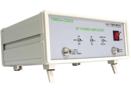
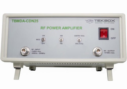
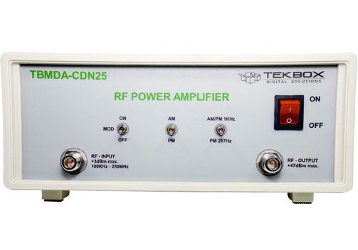
The TekBox TBMDA-CDN25 are modulated amplifier that provides the necessary power, bandwidth, and modulation for conducted immunity testing using CDNs and BCI probes in the frequency range from 100 kHz to 250 MHz. It is designed to be driven by signal generators or by tracking generators of spectrum analyzers. With a 1 dB compression point of up to 25 W in the frequency range 100 kHz to 250 MHz it can generate test levels class 1, class 2, class 3 and class X according to ISO/EN 61000-4-6. A built in AM/PM modulator enables use of tracking generators as signal source. The TBMDA-CDN25 has sufficient gain to achieve maximum output power with 0 dBm provided by a spectrum analyzer tracking generator. Besides 1 kHz, 80% AM, the TBMDA-CDN25 provides built in modulation capability to generate 1 kHz, 50% duty cycle PM signals. In PM mode, the TBMDA-CDN25 can also generate a 217 Hz Signal with 12.5% duty cycle in order to simulate mobile phone TDMA noise.
- CW amplifier (modulation off).
- 1 kHz, 80% AM modulation.
- 1 kHz, 50% duty cycle pulse modulation.
- 217 Hz, 12.5% duty cycle pulse modulation.
- Applications:
General-purpose wideband RF power amplifier.
Wideband RF power amplifier for conducted immunity testing driving CDNs or BCI-probes.
Wideband RF power amplifier for radiated immunity testing, driving near field probes.
Wideband RF power amplifier for radiated immunity testing, driving TEM cells.
Model Overview
| Model | TBMDA-CDN25 | |
| Input/output | 50 Ω, N female | |
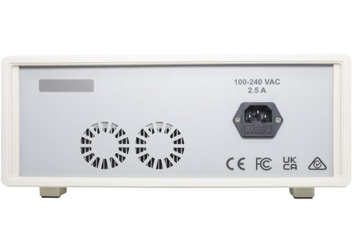
| Supply power range and consumption | 110...240 V; consumption 108 W at 220 V | |
| Operating temperature range | -20...50°C | |
| Frequency range | 100 kHz...250 MHz | |
| Small signal gain | 47 dB typ. | |
| Gain flatness | 100 kHz...250 MHz/Pin = -3 dBm: 3.5 dB typ. | |
| Saturated output power | 100 kHz/pin = 0 dBm | 44.1 dBm (25.7 W) typ. |
| 150 kHz/pin = 0 dBm | 44.6 dBm (28.8 W) typ. | |
| 500 kHz/pin = 0 dBm | 45.1 dBm (32.4 W) typ. | |
| 1 MHz/pin = 0 dBm | 45.3 dBm (33.9 W) typ. | |
| 10 MHz/pin = 0 dBm | 45.3 dBm (33.9 W) typ. | |
| 50 MHz/pin = 0 dBm | 45.6 dBm (36.3 W) typ. | |
| 80 MHz/pin = 0 dBm | 46.6 dBm (45.7 W) typ. | |
| 100 MHz/pin = 0 dBm | 46.5 dBm (44.7 W) typ. | |
| 150 MHz/pin = 0 dBm | 44.5 dBm (28.2 W) typ. | |
| 200 MHz/pin = 0 dBm | 43.8 dBm (24 W) typ. | |
| 230 MHz/pin = 0 dBm | 44.9 dBm (30.9 W) typ. | |
| 250 MHz/pin = 0 dBm | 44.8 dBm (30.2 W) typ. | |
| 1 dB output compression point | 100 kHz | +43.7 dBm typ. (pin: -5 dBm) |
| 150 kHz | +44.1 dBm typ. (pin: -4 dBm) | |
| 500 kHz | +44.6 dBm typ. (pin: -3 dBm) | |
| 1 MHz | +45 dBm typ. (pin: -3 dBm) | |
| 10 MHz | +45 dBm typ. (pin: -2 dBm) | |
| 50 MHz | +45.6 dBm typ. (pin: 1 dBm) | |
| 80 MHz | +46.5 dBm typ. (pin: 1 dBm) | |
| 100 MHz | +46.5 dBm typ. (pin: 0 dBm) | |
| 150 MHz | +42.9 dBm typ. (pin: -4 dBm) | |
| 200 MHz | +42.2 dBm typ. (pin: -4 dBm) | |
| 230 MHz | +44.1 dBm typ. (pin: -3 dBm) | |
| 250 MHz | +43 dBm typ. (pin: -4 dBm) | |
| Harmonics | 2nd harmonic, 100 MHz | Pout = 46 dBm: <–12 dBc typ. |
| 2nd harmonic, 100 MHz | Pout = 40 dBm: <–15 dBc typ. | |
| 3rd harmonic, 100 MHz | Pout = 46 dBm: <–22 dBc typ. | |
| 3rd harmonic, 100 MHz | Pout = 40 dBm: <–22 dBc typ. | |
| Total harmonic distortion | 17.7% at 100 MHz, Pout = 37 dBm typ. | |
| 19.6% at 100 MHz, Pout = 40 dBm typ. | ||
| 22.1% at 100 MHz, Pout = 43 dBm typ. | ||
| 26.9% at 100 MHz, Pout = 46 dBm typ. | ||
| Third order output intercept point: +51 dBm, at 100 MHz, Δf = 2 MHz, typ. | ||
| Internal modulation frequency AM: 1 kHz ±20% | ||
| Internal modulation frequencies PM: 1 kHz ±20%, 217 Hz ±20% | ||
| Duty cycle, PM: 50% ±10% at 1 kHz; 12.5% ±20% at 217 Hz | ||
| Maximum ratings | Max. input power +3 dBm; the output of the TBMDA-CDN25 is quite tolerant to output mismatch, however open or shorted load is not recommended, as it potentially can cause damage to the output transistor. When driving near field probes, current probes or any load of unknown impedance, it is highly recommended to insert a ≥3 dB attenuator at the output of the amplifier in order to protect the output stage. | |

Information on product safety:
Manufacturer:
TekBox Digital Solutions Vietnam Co. Ltd., Saigon Hi-Tech Park, Factory 4, 4F, Lot I-3B-1, N6 Street, Thu Duc City, 700 000 Ho Chi Minh City/VNM
www.tekbox.com
Responsible person:
Meilhaus Electronic GmbH, Am Sonnenlicht 2, 82239 Alling/DEU
info@meilhaus.com
Customers also bought


Last seen